 |
|---|
Nanotechnology at ECTI: Electron Beam Nanolithography Facility
By Dr. Aju Jugessur, ECTI
The Faculty’s Emerging Communications Technology Institute (ECTI) will give ‘birth’ to a new lab this fall: the Electron Beam Nanolithography Facility - the first one of its kind in Ontario and Western Canada.
The heart of this facility is a state-of-the-art, industry-grade Electron Beam Lithography system, EBPG5000+ fro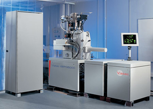 m Vistec Lithography Ltd. This technology can define features as small as 10 nm - about 2,000 times smaller than the width of a human hair.
To guarantee exceptional performance of the tool, this 108 m2 facility is being built in the basement of the Wallberg building, ensuring very low mechanical vibration (less than 10 µm/s), and the tool is enclosed in an environmental chamber maintaining stringent temperature control of 21 ± 0.25ºC at a maximum rate of change of 0.1ºC/hr.
It is enclosed in a Class 100 cleanroom environmental chamber, which means that the amount of dust and other particles is greatly reduced, providing a low-contaminant environment for research and device development. The facility also includes a new Class 100 cleanroom processing lab which will be used to process samples and wafers.
The possibilities to grow out of this initiative dedicated to the field of nanoscale science and engineering and nanofabrication are almost limitless. As Nobel laureate Richard Feynman noted almost 50 years ago, “When we get to the very, very small world – say circuits of seven atoms, we have a lot of new things that would happen that represent completely new opportunities for design.” ECTI's Electron Beam Nanolithography Facility will help U of T explore those opportunities.
In a nutshell, EBL is a specialized technique for creating extremely fine patterns at the submicron and nanometre scale. Derived from the early scanning electron microscopes, this technique consists of scanning a beam of electrons across a surface covered with an electron-sensitive film.
For several decades, EBL technology has been the primary technique for defining structures at the nanoscale. This technology is currently being used to define critical layers in electronic circuits used in computer chips. It is also used for the fabrication of optical masks in the integrated electronic circuit industry, and has applications in areas ranging from electronic devices and integrated optics to the emerging fields of nano-biotechnology, nano- electromechanical systems (NEMS), nanophotonics, nanomagnetics and nanoimprint.
This facility could be the convergence point for researchers from a number of science and engineering disciplines – demonstrating the versatility of the EBL technology and the multidisciplinary nature of nanotechnology research.
Funded with over $6 million from the Canada Foundation for Innovation, the Ontario Innovation Trust and the Ontario Research Fund, the facility will be accessible to both academic and industrial users for their Electron Beam Lithography requirements.
ECTI also offers users the next fabrication stage such as submicron etching and device characterization with the support of the other ECTI labs. ECTI now has the technological capability to explore new design and fabrication possibilities on the nanoscale for next-generation devices – driven by high pattern resolution and placement accuracy.
About ECTI
The Emerging Communications Technology Institute is an interdisciplinary open research facility based at the Faculty of Applied Science and Engineering, in the University of Toronto. ECTI promotes collaborative research with strategic partners from academia, government and industry. It also facilitates advanced educational opportunities and information exchange events. The Institute manages and operates the Open Research Facility consisting of several state-of-the-art research labs. These Labs enable research in the areas of nanotechnology and nanofabrication, photonic materials and devices, micro- and nano-electromechanical systems (M/NEMS), biotechnology, microwave devices, micro- and nano-electronic devices, integrated optics and photovoltaic devices. www.ecti.utoronto.ca